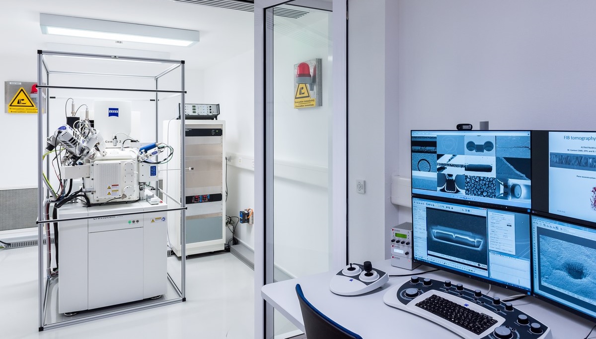
XB540 – it may look like the code name of a secret agent, but in fact it is a scientific tool used for nanoscale investigations at CERN. For the past year, this extraordinary machine – a focused ion beam scanning electron microscope (FIB-SEM) – has been digging beneath the surface to answer some long-standing questions in material science.
The XB540 FIB-SEM is an electron microscope and a 3D nano-machining workstation in one. While the high-resolution-scanning electron column can identify features as small as one millionth of a millimetre (10-9 m), or just about the size of ten atoms, it only shows the surface of a sample. The additional FIB column, on the other hand, uses an ion beam to cut through the matter and gives an insight into what lies underneath.
The machine makes 3D reconstructions of regions of interest in a process that resembles conventional tomography. The ion beam sequentially removes nanoscale slices of the material and an image of every new layer is made. Combining thousands of these images results in a precise 3D reconstruction of the internal structure of a sample.

"There was a real need for this microscope. It helps us understand phenomena that otherwise would have remained unexplained, either because of difficulties in preparation of the sample or due to limited resolution," says Stefano Sgobba from the Engineering department, leader of the Materials, Metrology and NDT section managing the scanning electron microscopy laboratory.
So far studies have been done on a diverse range of samples, including thin films, pressure vessels, structural materials, bulk assemblies, electrical components, insulating materials and beam-interaction samples.
The thin film experts from the Vacuum, Surfaces and Coatings group have been among the first to put the results to use. "For a long time, they wanted to associate different production parameters with the impact they have on the film. Up until now it has been very difficult to quantify this behaviour. They produced multiple samples with different parameters and we gave them an insight into the microstructure, the thickness and the porosity of each of them. Thanks to this information, they now know more about which production parameters are the most suitable," explains Alexander Lunt, who is responsible for managing and operating the FIB-SEM laboratory.
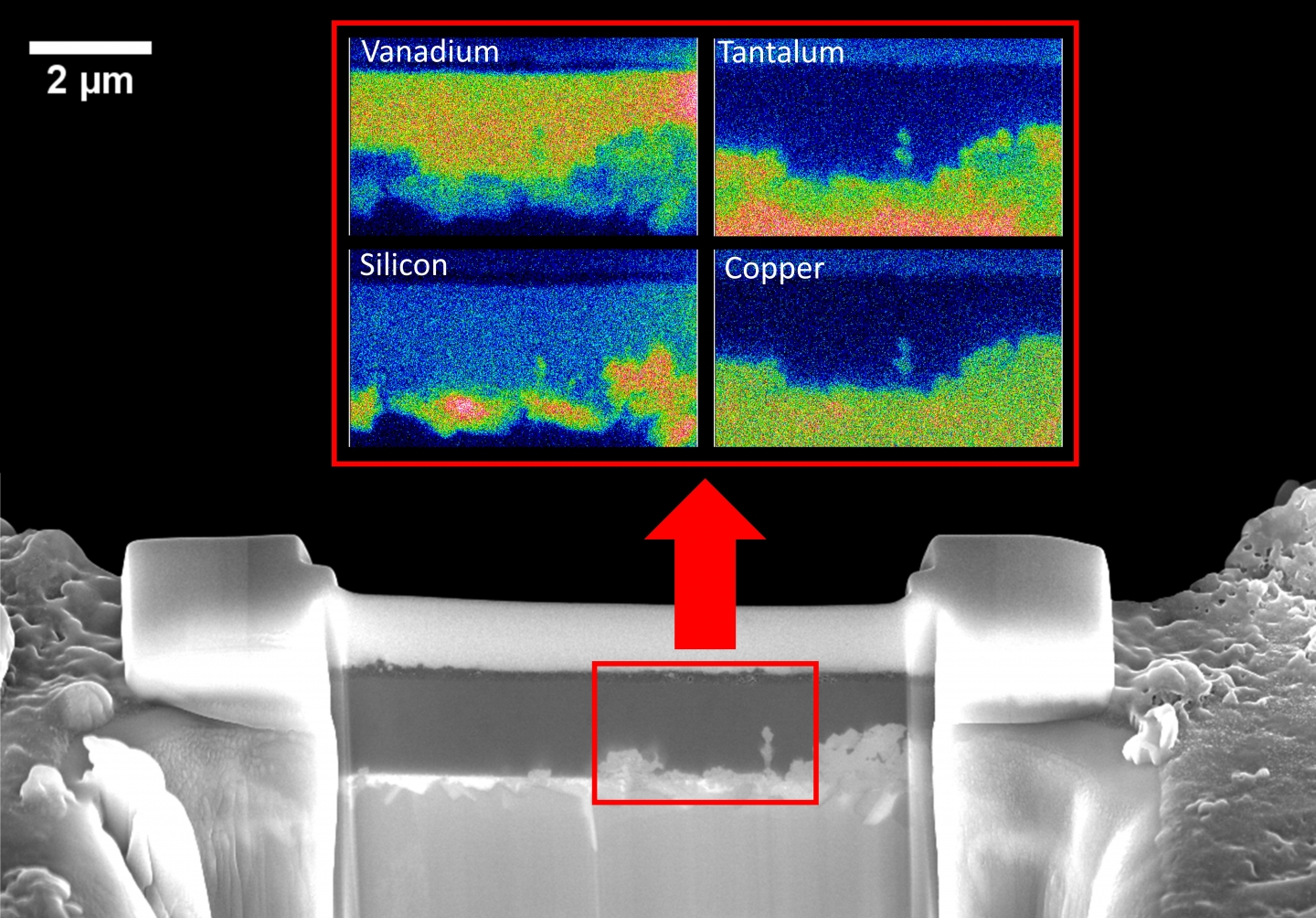
In addition to its milling and imaging functions, the microscope was also designed to perform different analysis techniques like elemental characterisation. Designated detectors inside are able to identify the elemental composition of the sample. "We know precisely what the material is made of, with very high resolution," says Floriane Léaux, who is responsible for electronic microscopy activity at CERN.
Another analysis technique is the production of a lamella – a small slice of the material, less than 200 nanometres thick. It allows the researchers to look through the sample at a resolution of 0.9 nanometres. "In a lamella we can see a plane of atoms that have become misaligned in the crystal and have formed a dislocation. This tells us what has to be optimised in the production technology to improve the final product," explains Alexander.

The Mechanical and Materials Engineering group drew up a specification and procured the FIB-SEM with support from other CERN departments and the Accelerator Consolidation project. Stefano adds: "We would like to thank everybody who supported us in this achievement. This situation clearly shows that there is a single unified community at CERN working to reach our specific scientific goals."

